NS 公司的ADC16V130是LVDS輸出的16位130MSPS高性能ADC,雙電源1.8V和3.0V工作,16位分辨率,取樣速率130MSPS,滿功率帶寬1.4GHz,160-MHz的SNR為76.7dB, SFDR為90.6dBFS,主要應用在高IF取樣接收器,多載波基站接收器,測試測量設備,通信基礎設備,數據采集和手提儀表等.本文介紹了ADC16V130主要特性,方框圖,低頻和高頻變壓器驅動電路以及SP16130CH4RB低IF接收器參考設計主要特性,詳細電路圖和材料清單(BOM).
ADC16V130: 16-Bit, 130 MSPS A/D Converter with LVDS Outputs
The ADC16V130 is a monolithic high performance CMOS analog-to-digital converter capable of converting analog input signals into 16-bit digital words at rates up to 130 Mega Samples Per Second (MSPS). This converter uses a differential, pipelined architecture with digital error correction and an onchip sample-and-hold circuit to minimize power consumption and external component count while providing excellent dynamic performance. Automatic power-up calibration enables excellent dynamic performance and reduces part-to-part variation, and the ADC16V130 could be re-calibrated at any time by asserting and then de-asserting power-down. An integrated low noise and stable voltage reference and differential reference buffer amplifier easies board level design. On-chip duty cycle stabilizer with low additive jitter allows wide duty cycle range of input clock without compromising its dynamic performance. A unique sample-and-hold stage yields a fullpower bandwidth of 1.4 GHz. The digital data is provided via full data rate LVDS outputs – making possible the 64-pin, 9mm x 9mm LLP package. The ADC16V130 operates on dual power supplies +1.8V and +3.0V with a power-down feature to reduce the power consumption to very low levels while allowing fast recovery to full operation.
ADC16V130主要特性:
■ Dual Supplies: 1.8V and 3.0V operation
■ On chip automatic calibration during power-up
■ Low power consumption
■ Multi-level multi-function pins for CLK/DF and PD
■ Power-down and sleep modes
■ On chip precision reference and sample-and-hold circuit
■ On chip low jitter duty-cycle stabilizer
■ Full data rate LVDS output port
■ 64-pin LLP package (9x9x0.8, 0.5mm pin-pitch)
ADC16V130主要指標:
■ Resolution 16 Bits
■ Conversion Rate 130 MSPS
■ SNR
(fIN = 10MHz)
(fIN = 70MHz)
(fIN = 160MHz)
78.5 dBFS (typ)
77.8 dBFS (typ)
76.7 dBFS (typ)
■ SFDR
(fIN = 10 MHz)
(fIN = 70MHz)
(fIN = 160MHz)
95.5 dBFS (typ)
92.0 dBFS (typ)
90.6 dBFS (typ)
■ Full Power Bandwidth 1.4 GHz (typ)
■ Power Consumption
Core
LVDS Driver
Total
650 mW (typ)
105 mW (typ)
755 mW (typ)
■ Operating Temperature Range -40°C ~ 85°C
ADC16V130應用:
■ High IF Sampling Receivers
■ Multi-carrier Base Station Receivers GSM/EDGE, CDMA2000, UMTS, LTE and WiMax
■ Test and Measurement Equipment
■ Communications Instrumentation
■ Data Acquisition
■ Portable Instrumentation
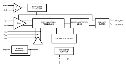
圖1.ADC16V130方框圖
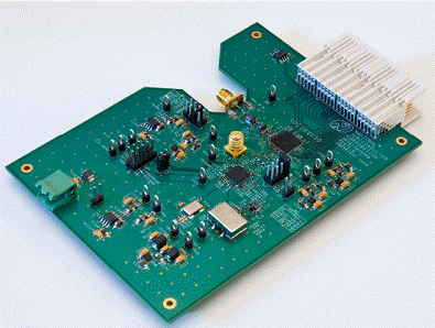
圖2. ADC16V130低頻輸入變壓器驅動電路
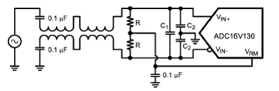
圖3. ADC16V130高頻輸入變壓器驅動電路
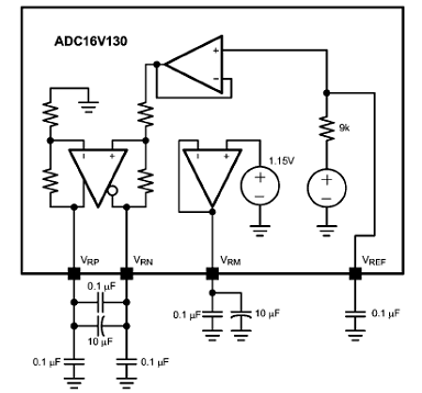
圖4. ADC16V130內部基準和去耦電路
SP16130CH4RB參考設計板
The SP16130CH4RB Reference Board demonstrates a low IF receiver subsystem application including an ADC16V130 analog-to-digital converter (ADC) and LMK04031B clock conditioner which provides digitization and clocking as used in wireless infrastructure systems.
This subsystem reference design provides single to differential conversion and lowpass filtering of the input signal with an optimized, double-balun network and high dynamic range digitization to parallel LVDS outputs using the ADC16V130. The 125 MHz low-jitter, LVPECL clock signal for the ADC is generated by a LMK04031B clock conditioner which demonstrates less than 250 fs of total jitter over the input bandwidth of the ADC.
The measured system performance demonstrates a large signal SNR of 75.8 dBFS and SFDR greater than 84 dBFS for a -1 dBFS, 52 MHz input signal and a sampling frequency of 125 MSPS. For small signals, the performance improves to 78.0 dBFS SNR and greater than 94 dBFS SFDR.
Evaluation of this reference board is simplified with the WaveVision 5.1 Data Capture Board and WaveVision 5 software.
SP16130CH4RB低IF接收器參考設計板主要特性:
Key Features of the SP16130CH4RB Low IF Receiver Reference Design Board
■ Demonstrates a subsystem architecture used in wireless infrastructure systems and
frequency domain analyzers
■ Configured for input frequencies between 5 and 52 MHz
■ Board comes fully assembled and tested
■ Single (+5V) supply needed
■ All ADC features can be exercised
■ Featured Products Include:
— ADC16V130 16-bit, 130 Megasample per second (MSPS) ADC with parallel LVDS outputs
— LMK04031B low-jitter precision clock conditioner consisting of cascaded phase locked loops (PLLs), an internal voltage controlled oscillator (VCO) and a distribution stage
— Several energy-efficient power management ICs
■ Large-signal (-1 dBFS) performance for a 52 MHz input signal:
— SNR = 75.8 dBFS
— SFDR > 84 dBFS
■ Small-signal (-20 dBFS) performance for a 52 MHz input signal:
— SNR = 78.0 dBFS
— SFDR > 94 dBFS
■ Total integrated jitter < 250 fs
■ PIC Loader board included with reference board for quick and easy configuration of the LMK04031B
■ Compatible with the WaveVision 5.1 Data Capture Board and WaveVision 5 software for simplified evaluation
圖5.低IF接收器參考設計板外形圖
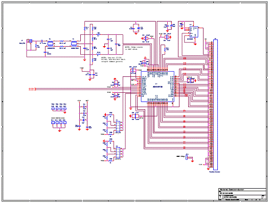
圖6.SP16130CH4RB電路圖: ADC
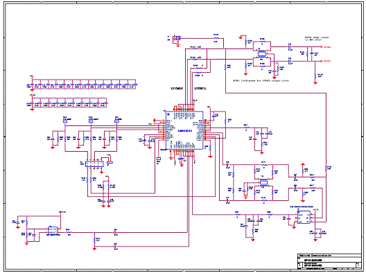
圖7.SP16130CH4RB電路圖: LMK
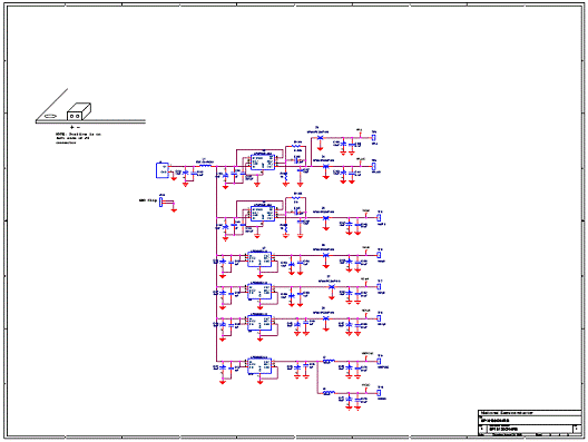
圖8SP16130CH4RB電路圖:電源
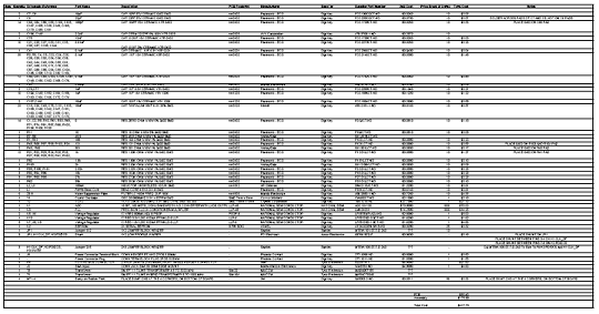
8SP16130CH4RB材料清單:
詳情請見:
http://www.national.com/ds/DC/ADC16V130.pdf
和
http://webench.national.com/rd/RD/RD-170.pdf
ADC16V130: 16-Bit, 130 MSPS A/D Converter with LVDS Outputs
The ADC16V130 is a monolithic high performance CMOS analog-to-digital converter capable of converting analog input signals into 16-bit digital words at rates up to 130 Mega Samples Per Second (MSPS). This converter uses a differential, pipelined architecture with digital error correction and an onchip sample-and-hold circuit to minimize power consumption and external component count while providing excellent dynamic performance. Automatic power-up calibration enables excellent dynamic performance and reduces part-to-part variation, and the ADC16V130 could be re-calibrated at any time by asserting and then de-asserting power-down. An integrated low noise and stable voltage reference and differential reference buffer amplifier easies board level design. On-chip duty cycle stabilizer with low additive jitter allows wide duty cycle range of input clock without compromising its dynamic performance. A unique sample-and-hold stage yields a fullpower bandwidth of 1.4 GHz. The digital data is provided via full data rate LVDS outputs – making possible the 64-pin, 9mm x 9mm LLP package. The ADC16V130 operates on dual power supplies +1.8V and +3.0V with a power-down feature to reduce the power consumption to very low levels while allowing fast recovery to full operation.
ADC16V130主要特性:
■ Dual Supplies: 1.8V and 3.0V operation
■ On chip automatic calibration during power-up
■ Low power consumption
■ Multi-level multi-function pins for CLK/DF and PD
■ Power-down and sleep modes
■ On chip precision reference and sample-and-hold circuit
■ On chip low jitter duty-cycle stabilizer
■ Full data rate LVDS output port
■ 64-pin LLP package (9x9x0.8, 0.5mm pin-pitch)
ADC16V130主要指標:
■ Resolution 16 Bits
■ Conversion Rate 130 MSPS
■ SNR
(fIN = 10MHz)
(fIN = 70MHz)
(fIN = 160MHz)
78.5 dBFS (typ)
77.8 dBFS (typ)
76.7 dBFS (typ)
■ SFDR
(fIN = 10 MHz)
(fIN = 70MHz)
(fIN = 160MHz)
95.5 dBFS (typ)
92.0 dBFS (typ)
90.6 dBFS (typ)
■ Full Power Bandwidth 1.4 GHz (typ)
■ Power Consumption
Core
LVDS Driver
Total
650 mW (typ)
105 mW (typ)
755 mW (typ)
■ Operating Temperature Range -40°C ~ 85°C
ADC16V130應用:
■ High IF Sampling Receivers
■ Multi-carrier Base Station Receivers GSM/EDGE, CDMA2000, UMTS, LTE and WiMax
■ Test and Measurement Equipment
■ Communications Instrumentation
■ Data Acquisition
■ Portable Instrumentation
圖1.ADC16V130方框圖
圖2. ADC16V130低頻輸入變壓器驅動電路
圖3. ADC16V130高頻輸入變壓器驅動電路
圖4. ADC16V130內部基準和去耦電路
SP16130CH4RB參考設計板
The SP16130CH4RB Reference Board demonstrates a low IF receiver subsystem application including an ADC16V130 analog-to-digital converter (ADC) and LMK04031B clock conditioner which provides digitization and clocking as used in wireless infrastructure systems.
This subsystem reference design provides single to differential conversion and lowpass filtering of the input signal with an optimized, double-balun network and high dynamic range digitization to parallel LVDS outputs using the ADC16V130. The 125 MHz low-jitter, LVPECL clock signal for the ADC is generated by a LMK04031B clock conditioner which demonstrates less than 250 fs of total jitter over the input bandwidth of the ADC.
The measured system performance demonstrates a large signal SNR of 75.8 dBFS and SFDR greater than 84 dBFS for a -1 dBFS, 52 MHz input signal and a sampling frequency of 125 MSPS. For small signals, the performance improves to 78.0 dBFS SNR and greater than 94 dBFS SFDR.
Evaluation of this reference board is simplified with the WaveVision 5.1 Data Capture Board and WaveVision 5 software.
SP16130CH4RB低IF接收器參考設計板主要特性:
Key Features of the SP16130CH4RB Low IF Receiver Reference Design Board
■ Demonstrates a subsystem architecture used in wireless infrastructure systems and
frequency domain analyzers
■ Configured for input frequencies between 5 and 52 MHz
■ Board comes fully assembled and tested
■ Single (+5V) supply needed
■ All ADC features can be exercised
■ Featured Products Include:
— ADC16V130 16-bit, 130 Megasample per second (MSPS) ADC with parallel LVDS outputs
— LMK04031B low-jitter precision clock conditioner consisting of cascaded phase locked loops (PLLs), an internal voltage controlled oscillator (VCO) and a distribution stage
— Several energy-efficient power management ICs
■ Large-signal (-1 dBFS) performance for a 52 MHz input signal:
— SNR = 75.8 dBFS
— SFDR > 84 dBFS
■ Small-signal (-20 dBFS) performance for a 52 MHz input signal:
— SNR = 78.0 dBFS
— SFDR > 94 dBFS
■ Total integrated jitter < 250 fs
■ PIC Loader board included with reference board for quick and easy configuration of the LMK04031B
■ Compatible with the WaveVision 5.1 Data Capture Board and WaveVision 5 software for simplified evaluation
圖5.低IF接收器參考設計板外形圖
圖6.SP16130CH4RB電路圖: ADC
圖7.SP16130CH4RB電路圖: LMK
圖8SP16130CH4RB電路圖:電源
8SP16130CH4RB材料清單:
詳情請見:
http://www.national.com/ds/DC/ADC16V130.pdf
和
http://webench.national.com/rd/RD/RD-170.pdf
 粵公網安備 44030902003195號